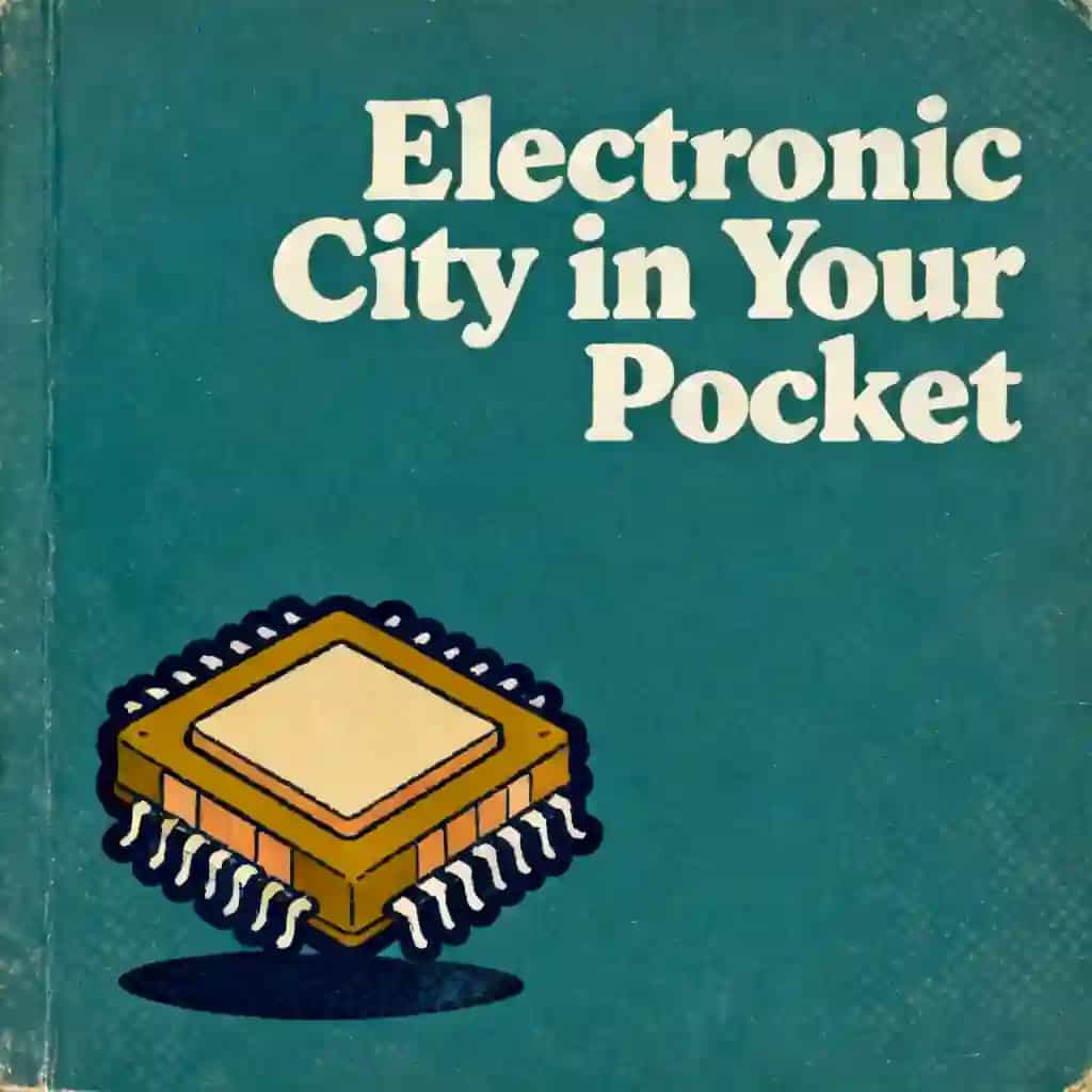
Integrated Circuit: History, Design, and Semiconductor Technology
Explore the history and design of integrated circuits. Learn about semiconductor technology, VLSI, and how silicon chips and transistors power modern electronics.

Best quote from Integrated Circuit: History, Design, and Semiconductor Technology
It’s the ultimate human achievement in manufacturing—taking the most common material on earth, sand, and through pure engineering will, turning it into something that can calculate billions of times a second.
Generated by Gerardo Valdez
Integrated circuit

Frequently Asked Questions
An integrated circuit, often called a microchip or silicon chip, is a set of electronic circuits on a small flat piece of semiconductor material. These components are fundamental to modern semiconductor technology because they allow for the miniaturization of complex electronics. By integrating thousands or millions of tiny transistors into a single chip, integrated circuits enable the functionality of everything from smartphones to advanced computing systems.
The evolution of the transistor is the cornerstone of microchip design history. Originally developed as individual components, the transition to embedding multiple transistors onto a single substrate revolutionized the industry. This shift allowed for higher efficiency and lower power consumption. Over decades, the ability to shrink these transistors has led to the development of Very Large Scale Integration (VLSI), which defines the high-performance chips we use today.
Very Large Scale Integration, or VLSI, is the process of creating an integrated circuit by combining millions or even billions of MOS transistors into a single chip. This technology is a critical aspect of microchip design, as it allows for the creation of powerful microprocessors and memory devices. VLSI has been the driving force behind the rapid advancement of silicon chips, making complex computing tasks accessible in portable devices.
From Columbia University alumni built in San Francisco
"Instead of endless scrolling, I just hit play on BeFreed. It saves me so much time."
"I never knew where to start with nonfiction—BeFreed’s book lists turned into podcasts gave me a clear path."
"Perfect balance between learning and entertainment. Finished ‘Thinking, Fast and Slow’ on my commute this week."
"Crazy how much I learned while walking the dog. BeFreed = small habits → big gains."
"Reading used to feel like a chore. Now it’s just part of my lifestyle."
"Feels effortless compared to reading. I’ve finished 6 books this month already."
"BeFreed turned my guilty doomscrolling into something that feels productive and inspiring."
"BeFreed turned my commute into learning time. 20-min podcasts are perfect for finishing books I never had time for."
"BeFreed replaced my podcast queue. Imagine Spotify for books — that’s it. 🙌"
"It is great for me to learn something from the book without reading it."
"The themed book list podcasts help me connect ideas across authors—like a guided audio journey."
"Makes me feel smarter every time before going to work"


![[3ef8aafc-ee48-42ad-951e-2912ec070073:c0001] I'm back with Reiner Pope, CEO of MatX, a new AI chip com… p1-1](/_next/image?url=https%3A%2F%2Fd1y2du6z1jfm9e.cloudfront.net%2Fassets%2Fpodcast%2Fblue.png&w=1024&q=50)